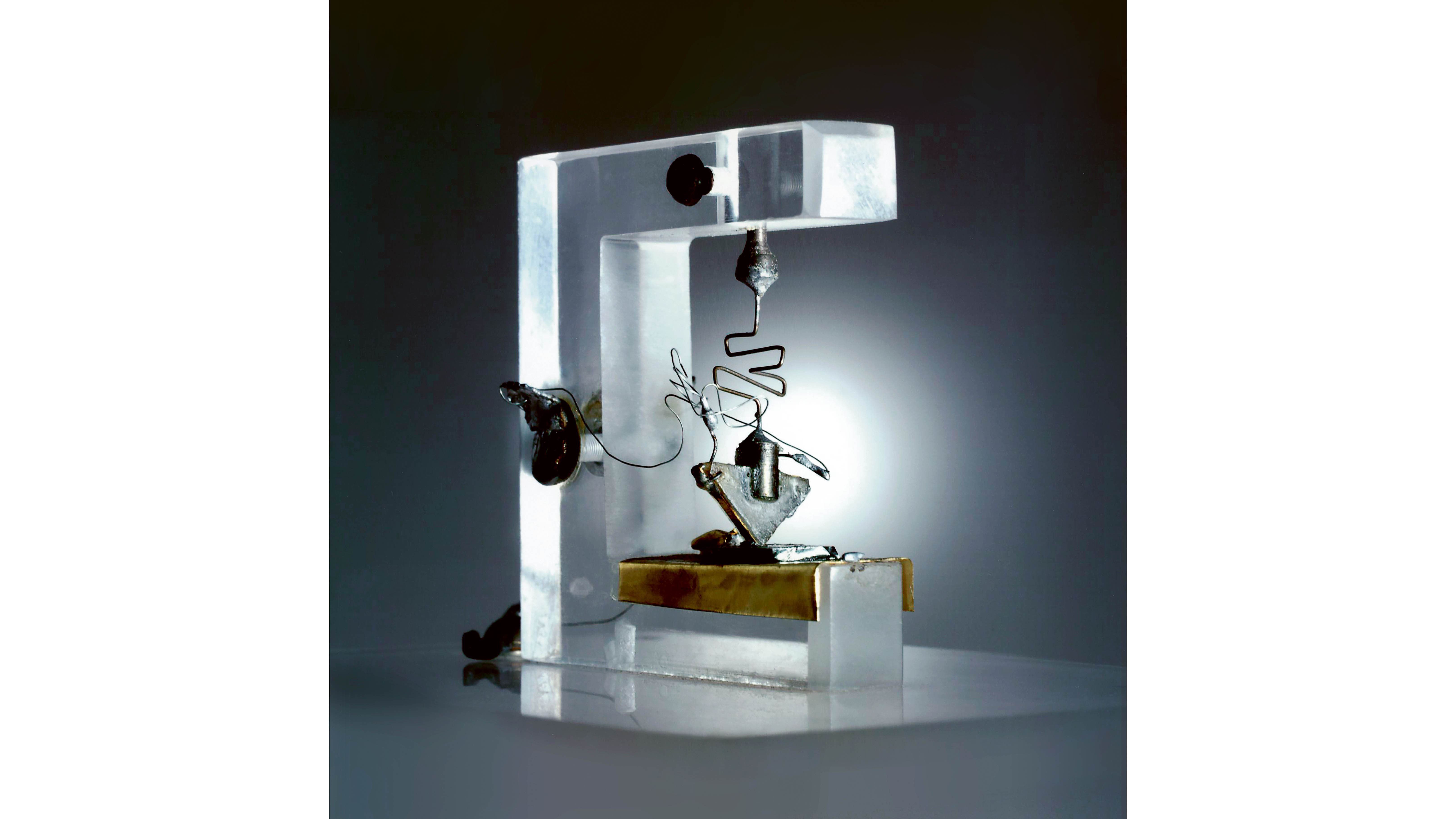
The birth of modern electronics took place on December 16, 1947 at Bell Labs in Murray Hill, New Jersey. It was then that physicist Walter Brattain succeeded for the first time in amplifying an electric voltage with an improvised semiconductor component. The transistor was born. For the first time, an alternative to the bulky, unreliable, and energy-hungry vacuum tubes was available. From an appearance standpoint, Brattain’s laboratory setup, consisting of a germanium plate, a plastic triangle, gold foil, and a paper clip, had very little in common with modern chips – but it did herald the era of personal computers, smartphones, and self-propelled cars.
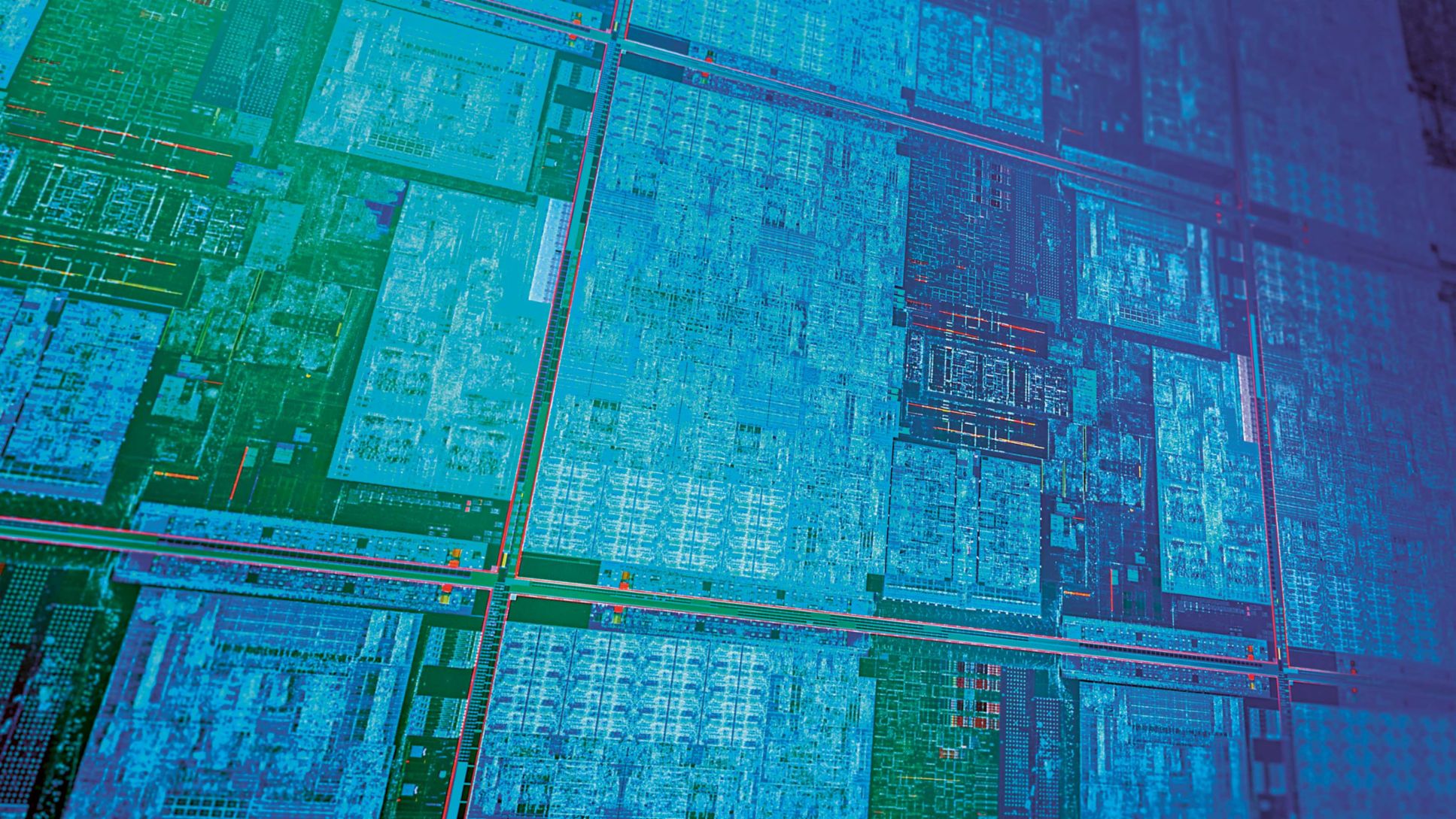
The new electronic component could be used as an amplifier and as a switch – and together with its peers and other components such as resistors and capacitors, it could be accommodated as an integrated circuit (IC) on a single semiconductor wafer. In the decades that followed, semiconductor companies succeeded in making the components ever smaller and accommodating an ever greater number of them on the same surface. As early as 1965, Gordon Moore predicted that the number of transistors per unit area would increase exponentially.
Simple scaling reaches its limits
Moore’s prediction has proven to be essentially correct over decades. But now it is finally reaching its limits, because the gradual reduction in size of the proven MOSFETs (Metal-Oxide-Semiconductor Field-Effect Transistor) as switches on the chips no longer works: “About 15 years ago, people realized that simple scaling had reached its limits,” reports Dr. Heike Riel, IBM Fellow at the IBM Research Center in Rüschlikon, Switzerland. “That’s why manufacturers first replaced silicon dioxide as the insulating material in the transistors with so-called High-K materials while retaining the same MOSFET geometry. This made it possible to produce chips with structures 45 nm in size.”
But even this trick could only keep Moore’s Law alive for a few years. For this reason, chip manufacturers began using a new transistor architecture for even smaller components in the first half of the 2010s: the FinFET. The conductive channel between the source and drain terminals is shaped like a fin and is enclosed on several sides by the gate. “This makes it much easier to control the current flow in the transistor,” says Riel. “FinFETs starting at 22 nm in structure size were used and are now standard in integrated circuits.”
The gate-all-around FET
But their successor is also already available. Starting at structure sizes of five nanometers, the GAAFET (gate-all-around FET) will take over the work in the chips. “In the GAAFET, the conductive channel between source and drain consists of several parallel silicon nanowires, each of which is completely enclosed by the gate electrode,” explains Riel. “This is the optimal geometry for controlling the current flow. It also saves space on the chips because several of these nanowire structures, which form the channel of the transistor, are superimposed on each other.” Automotive applications will also benefit from developments such as GAAFET in the future – because both the new, powerful High Performance Computing Platforms (HCPs) as successors to the many decentralized control units and the special processors for autonomous driving depend on chips with high computing power. However, even GAAFET won’t be able to save Moore’s Law in the long run: beyond a structure size of three nm, things will get tight.This limit could be reached in three to four years.
“An ingenious phase of improvement is thus coming to an end,” says Prof. Thomas Schimmel, Director at the Institute of Nanotechnology at the Karlsruhe Institute of Technology (KIT). “Until now, a technical solution has always been found that enabled further miniaturization of the classic transistor – but now atomic dimensions have been reached in the chips. Thanks to the quantum mechanical tunnel effect, electrons can pass through insulators, which would render the components useless. This is because, contrary to the ideas of classical physics, the electrons can overcome barriers even when they do not actually have enough energy to do so.” But even the targeted introduction of foreign atoms into the highly pure silicon during the production process – a procedure known as “doping” – no longer functions reliably with ever smaller structures.
No clear successor in sight
The search is therefore on for a successor to the transistor that will further increase the performance of electronic circuits in the future. IBM researcher Riel lists a whole range of MOSFET alternatives, including the carbon nanotube field-effect transistor (CNFET) and the tunnel FET (TFET). In the CNFET, current flows through tiny carbon tubes. This year, researchers from MIT have shown that the fast and energy-efficient switches can be produced in conventional chip factories. TFETs are similar in design to conventional transistors, but put the quantum mechanical tunnel effect to their advantage for switching. They are energy-saving and fast. Whether CNFET, TFET, or any other approach will win the race is completely open. “There is currently a lot of research, but no clear front-runner to succeed the optimized silicon MOSFET,” says Riel.
KIT researcher Schimmel is therefore betting on the single-atom transistor in the long term: in this transistor, a control electrode shifts an atom that can close the tiny gap between two terminals and thus enable the flow of current. “In principle, it works like a relay with two stable states,” says Schimmel, who developed the first single atom transistor with his team in 2004. “This makes the single-atom transistor not only a switch, but also a non-volatile memory. It could also replace conventional RAM chips as the main memory in computers. Since it retains its state even without power, computers would no longer have to be restarted in the future, but could continue working immediately after a break.”
“There is currently a lot of research, but no front-runner to succeed the optimized silicon MOSFET.” Dr. Heike Riel, IBM
Another advantage is that the single-atom transistor requires significantly less voltage than the MOSFET and would therefore only consume about one ten-thousandth of the energy per switching operation. This would solve the heat problem in today’s chips, and clock frequencies of up to 100 gigahertz would be within reach. Schimmel has already built a first IC with two of his novel transistors, and for a later series production a mix of proven processes of the semiconductor industry and galvanic procedures could be used. “It’s like galvanizing a car body – only on an atomic scale,” says the Karlsruhe scientist.
New chip and computer architectures
As an alternative to the ever-advancing miniaturization of components, new approaches to chip architecture are also possible, for example the path into the third dimension: in order to pack more power into the circuits, several electronic layers could be stacked on top of each other – already practiced today with flash memories. In the future, manufacturers could also apply a layer of compound semiconductors, as they are known, such as indium gallium arsenide (InGaAs) to a layer of conventional silicon transistors.
They are suitable for special tasks such as particularly fast amplification, for the emission or detection of light, and also as possible quantum components. Many experts are counting on the integration of such additional functions into the chips to compensate for the demise of Moore’s Law. They’re taking a new approach: instead of “more Moore” (further miniaturization), they prefer “more than Moore” (the combination of digital and non-digital functions on the same chip).
The in-memory computing
In-memory computing, which is intended to eliminate the spatial separation of the computing unit and memory in common computers, promises much higher computing power and energy efficiency. This would eliminate the time-consuming and energy-intensive transport of bytes between microprocessor and RAM. For example, the vector-matrix calculations in a neural network can be performed using a crossbar architecture – analog rather than digital. In this approach, two bundles of horizontal and vertical lines cross, each of which acts as an input and output of the neural network. At their intersection points, the lines are connected to each other via non-volatile memory elements that represent the weighting factors (the “knowledge”) of the neural network. The input values of the neural network are applied as analog voltage values to the horizontal lines. The results of the calculations are available almost instantaneously on the vertical lines, also in analog form – and without any data transport.
Non-volatile memories at the crossing points of the lines include memristors, novel electronic components whose resistance can be permanently changed by an externally applied voltage and which can be combined with existing manufacturing processes in the semi-conductor industry. Memristors can be used to perform calculations in neural networks ten to a hundred times faster, depending on the application, and their energy efficiency can also be improved by a factor of ten to a thousand. Autonomous vehicles in which neural networks play a major role could also benefit from such performance and efficiency improvements. The example shows that even if Moore’s Law soon reaches its limits, the continuous increase in performance of electronics is far from over.
MOSFET, FinFET and GAAFET
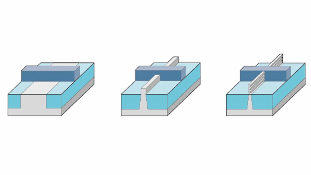
The MOSFET (left) has been the workhorse switch for digital technology for decades and has kept Moore’s Law alive through its continual miniaturization. The voltage between the gate and source electrode determines the current flowing through the channel from source to drain. In the FinFET (center), the channel has the shape of a fin so that the gate can surround it on three sides. This improves current flow control compared to the MOSFET, where the gate can only act on the channel from above. In the GAAFET (right), the gate completely encloses the channel of silicon nanowires. This is the optimal geometry for controlling the current flow.
Future alternatives to the conventional transistor design
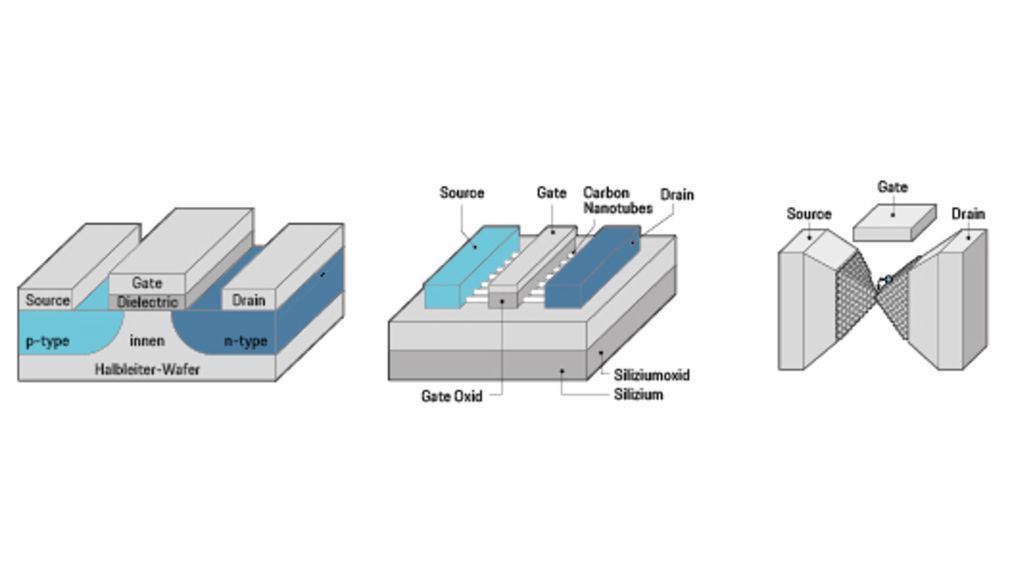
In the TFET (left), unlike the MOSFET, the source and drain are differently doped. It uses the quantum mechanical tunnel effect: the voltage between gate and source determines whether charge carriers can “tunnel” through the energetic barrier between source and drain and whether a current flow is possible. In the CNFET (center), the channel between source and drain consists of carbon nanotubes. Here too, the gate-source voltage determines the current flow. In the single-atom transistor (right), the voltage between source and gate shifts a single atom, which either closes or opens the circuit between source and drain (green/red position).
Moore's Law
55 years ago Gordon Moore made a remarkable prediction in Electronics magazine: the then-research director of Fairchild Semiconductor and later Intel co-founder in 1965 asserted that the number of transistors per chip would double every year in the future. As early as 1975, it would therefore be possible to accommodate around 65,000 of them on a tiny silicon wafer. “Moore’s Law" has been continually tweaked over the years, but has proven to be correct in principle and has become the guideline for semiconductor manufacturers: To this day, they have repeatedly succeeded in doubling the number of transistors per unit area at short intervals. In the future, however, this will no longer be possible. A higher performance of the chips must then be achieved by other means.
In brief
The further miniaturization of the MOSFET transistor and its variants FinFET and GAAFET is likely to reach its limits in the coming years. In order to make chips increasingly powerful in the future, research scientists and industry are working on new transistor designs such as tunnel FETs, as well as on new architectures such as in-memory computing.
Info
Text: Christian Buck
Text first published in the Porsche Engineering Magazine, issue 1/2021